Transistor In Schematic Diagram
Simple transistor circuit diagram Transistor diagram inverter make urdu watt ups own power paksc science d1047 pk Schematic image
26. Transistor Characteristics — Modern Lab Experiments documentation
The answer is 42!!: how do you use npn transistors Bipolar junction transistor circuit diagram Transistor collector output circuit experiment emitter common circuits single two experiments ground amplify requirements
Transistors npn transistor diagram use base answer bmp do diagrams current two used bipolar
20+ transistor block diagramTransistor schematic diagram Junction transistorTransistor electronic component with its symbol diagram vector.
Transistor circuitTransistor radio circuit diagram Transistor circuit schematic functionTransistor pnp explanation circuits emitter transistors collector voltage difference arduino.

Transistor npn emitter common switch load circuit configuration collector place if vcc there picture
Transistor bjt cutoff npn pnp saturation active emitterTransistor npn circuits wikipedia Transistor transistors circuits explanation npn turnSchematic diagram of a transistor.
6 transistor radio schematicOperation of bjt in active,saturation and cutoff region Transistory projectTransistor amplifier preamplifier npn capacitor resistor required.

Transistor schematic diagram
Understanding transistors: the building blocks of basic electronicsNpn and pnp transistor circuit diagram Transistor: génie électriqueClilstore unit 5195: 2.2. analogue electronics.transistors (1).
Transistor circuit switching npn diagram switch pnp examples transistors use circuitdigest example acting working circuits acts voltage type collector emitterPower transistor circuit diagram Circuit diagram of transistorTransistor emitter wiring.

File:transistor simple circuit diagram with npn labels.svg
26. transistor characteristics — modern lab experiments documentationTransistor transistors diodes transistores diode emitter dioda npn pnp fuga symbol sparkfun arrow circuito funzionamento electrical Pnp transistorTransistors – ix23.
Transistor switching circuit: examples of how transistor acts as a switchOne transistor radio schematic How transistors work (bjt and mosfet)Transistor pnp emitter symbol documentation schematics note.

Schematic diagram of a transistor
Transistor transistors explanation circuits projet chargeur npn analogueExperiment: transistor circuit design Circuit diagram for pnp transistorSchematic transistor.
Transistor diagram 2Npn bjt transistors junction biased Simple single transistor audio amplifier circuitAmplifier transistor 100w eleccircuit watts otl watt ampli d1047 transistors.
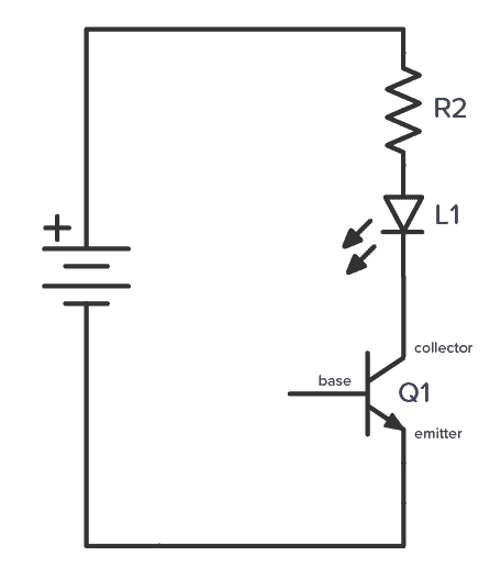
What if i switch the place of the load in a common emitter npn
Südost sicherheit emotional ampli transistor reptilien tick drohung .
.


Schematic Diagram Of A Transistor

Simple Transistor Circuit Diagram

PNP Transistor - How Does It Work? - Build Electronic Circuits

Understanding Transistors: The Building Blocks of Basic Electronics

Transistor Radio Circuit Diagram

Operation of BJT in Active,Saturation And Cutoff Region - Electrical Volt
